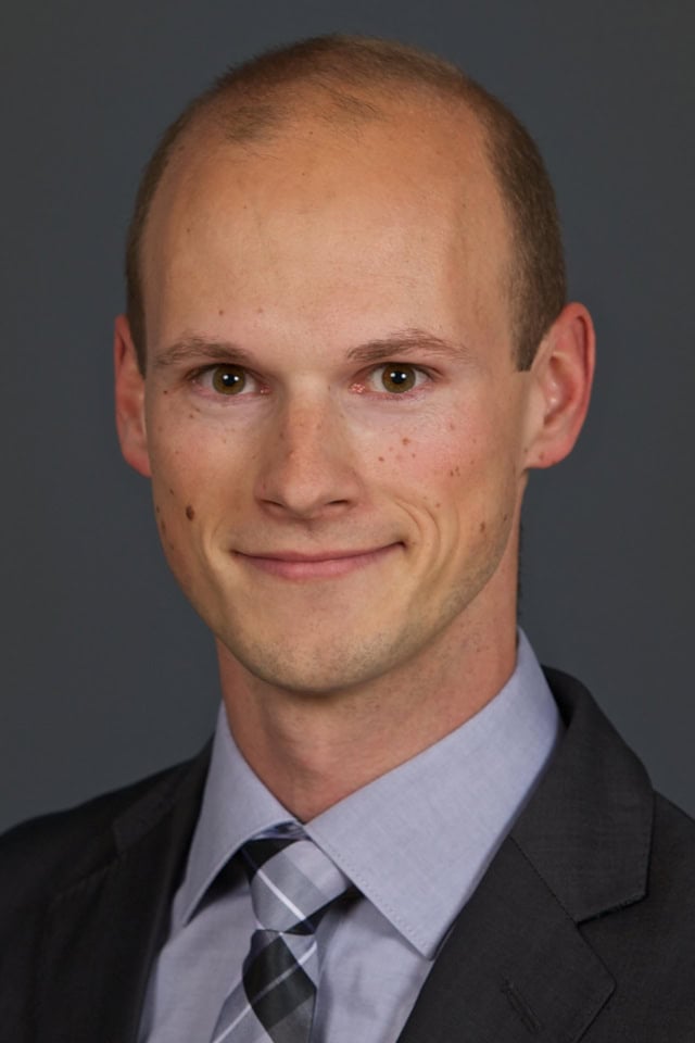
Peter J. Imrich is the head of the Materials Science & Simulation group at KAI Kompetenzzentrum Automobil- und Industrieelektronik GmbH, a multidisciplinary research center of Infineon Technologies Austria AG in Villach.
He obtained his PhD in Materials Science at the Montanuniversität Leoben, Austria in 2015, investigating the micro- and nanomechanical behavior of single- and bicrystalline copper samples in the scanning and transmission electron microscope.
After his graduation and a short post-doc position he joined Infineon Technologies Austria AG in Villach, working on technology-, site- and frontend/backend-overarching metallization topics, dealing with technical research projects, problem solving, complexity management and metallization roadmaps.
In 2021 he joined KAI GmbH, where he and his group are focusing on the development of advanced materials characterization and simulation techniques within Austrian and European funded research projects.
Pushing the limits in space and time using advanced synchrotron characterization techniques for microelectronics applications
Power electronics are continuously facing harsher requirements in application and the constant need of improving efficiency. This manifests in the need of more robust materials with respect to thermomechanical fatigue, structures with higher breakage strength and new devices based on III/V semiconductors. To ensure manufacturability, reliability and functionality of future power electronic devices, advanced characterization techniques are necessary to identify materials behaviour with high spatial (down to tens of nanometres) and temporal resolution (down to nanoseconds).
Three use cases will be presented to illustrate the potential of X-ray based synchrotron techniques. The first focuses on the characterization of thermomechanical fatigue in 20µm thick copper layers, which endure temperature pulses that heat the device locally above 300°C in roughly 200 µs, as common heat dissipation mechanisms via the packaging become ineffective [1]. To identify the mechanical materials response during these ultra-fast heating rates (up to 106 K) in-situ 20 kHz X-ray diffraction was utilized at the MS-Powder beamline of the Paul Scherrer Institute in Switzerland. Following this, the microstructural evolution responsible for Cu fatigue was investigated using in-situ dark field X-ray microscopy (DFXM) at the ID03 and ID06 beamlines of the European Synchrotron Radiation Facility (ESRF) in France. During this investigation, several hundred heat pulses were applied to track the changes in intragranular strain and misorientation within a single Cu grain throughout the thermo-mechanical cycling process.
The second use case investigates the sidewalls of silicon dies after laser dicing. Here nanobeam X-ray diffraction proves as a capable method to spatially resolve changes in the microstructure, element distribution and residual stresses in the recast layer at the chip sidewall. The experiments reveal the distribution and incorporation of elements from the backside metallization in the recast layer and their influence on microstructure and residual stresses. These results are compared with die breakage strength measurements as well as TEM investigations.
The final use case combines the high spatial and temporal resolution to shed light on the electrical operation of a GaN high electron mobility transistor (HEMT) during fast switching. The piezoelectric properties inherent to the GaN wurtzite crystal structure cause significant lattice strain to develop during hard switching of the device due to rapid changes in the electric field. This phenomenon can be exploited to enable real-time visualization of the local electric field within the active region of the device by investigating the time resolve lattice strain. In operando DFXM measurements were conducted at the ID01 beamline of the ESRF, providing a detailed mapping of the piezoelectric strain field during device switching with a temporal resolution of 1 ns and a spatial resolution of approximately 150 nm.
References
[1] S. Moser, M. Kleinbichler, J. Zechner, M. Reisinger, M. Nelhiebel, and M. J. Cordill, “Fatigue of copper films subjected to high-strain rate thermo-mechanical pulsing,” Microelectron. Reliab., vol. 137, p. 114782, Oct. 2022, doi: 10.1016/j.microrel.2022.114782.